Reuters 3000 keypad
I recently obtained the keypad section from a Reuters 3000 Xtra keyboard. I’m a fan of tiny keyboards like the planck. These keyboards usually don’t have a numpad, so an external keypad is appealing to me.
Discovery⌗
To start of with we will take a physical overview of this keypad. Both to learn what we have to work with, but also just to document it.
Description of the keypad⌗
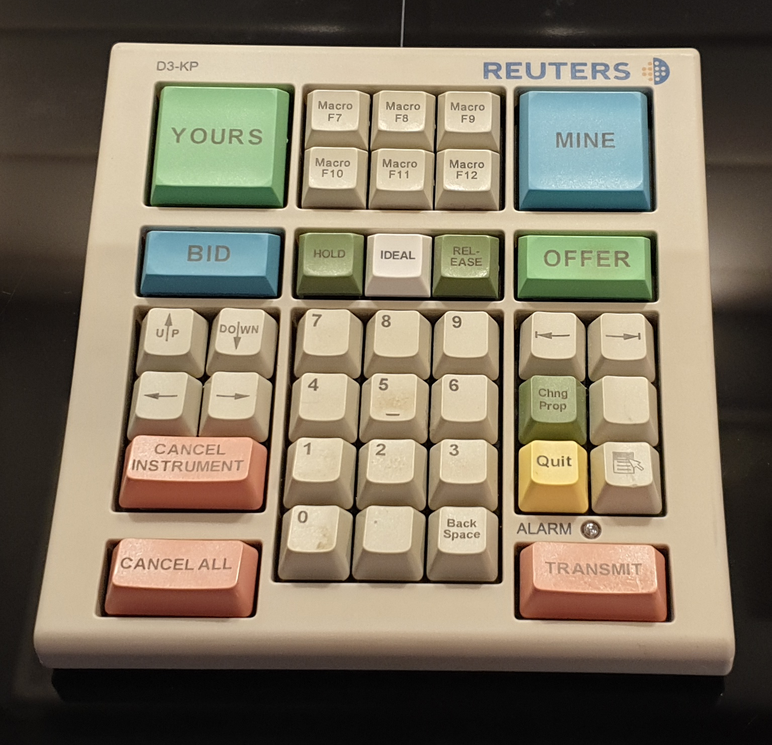
On the outside the first thing that catches the eye are the giant colored MINE and YOURS buttons, quickly followed by the other weirdly labeled and colored buttons. I’m sure they were meaningful in the 3000 Xtra system. I will make good use of them as macro buttons. Also notice the alarm label, behind that white cover is an led. I’m probably going to place the numlock indicator there.
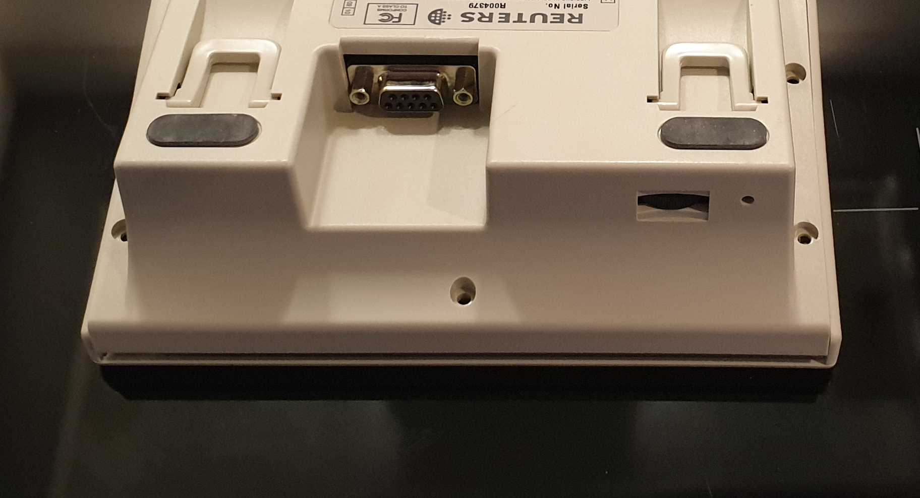
The back of the keyboard includes a hole for an internal button, a potentiometer dial, and the DSub-9 connector that originally connected the keyboard to the computer (or maybe some breakout box), I’ll have to adapt that to USB. The internal button could be useful for a hardware reset button when developing firmware, and the potentiometer could be fun as well. I’ll be looking to keep both of these working.
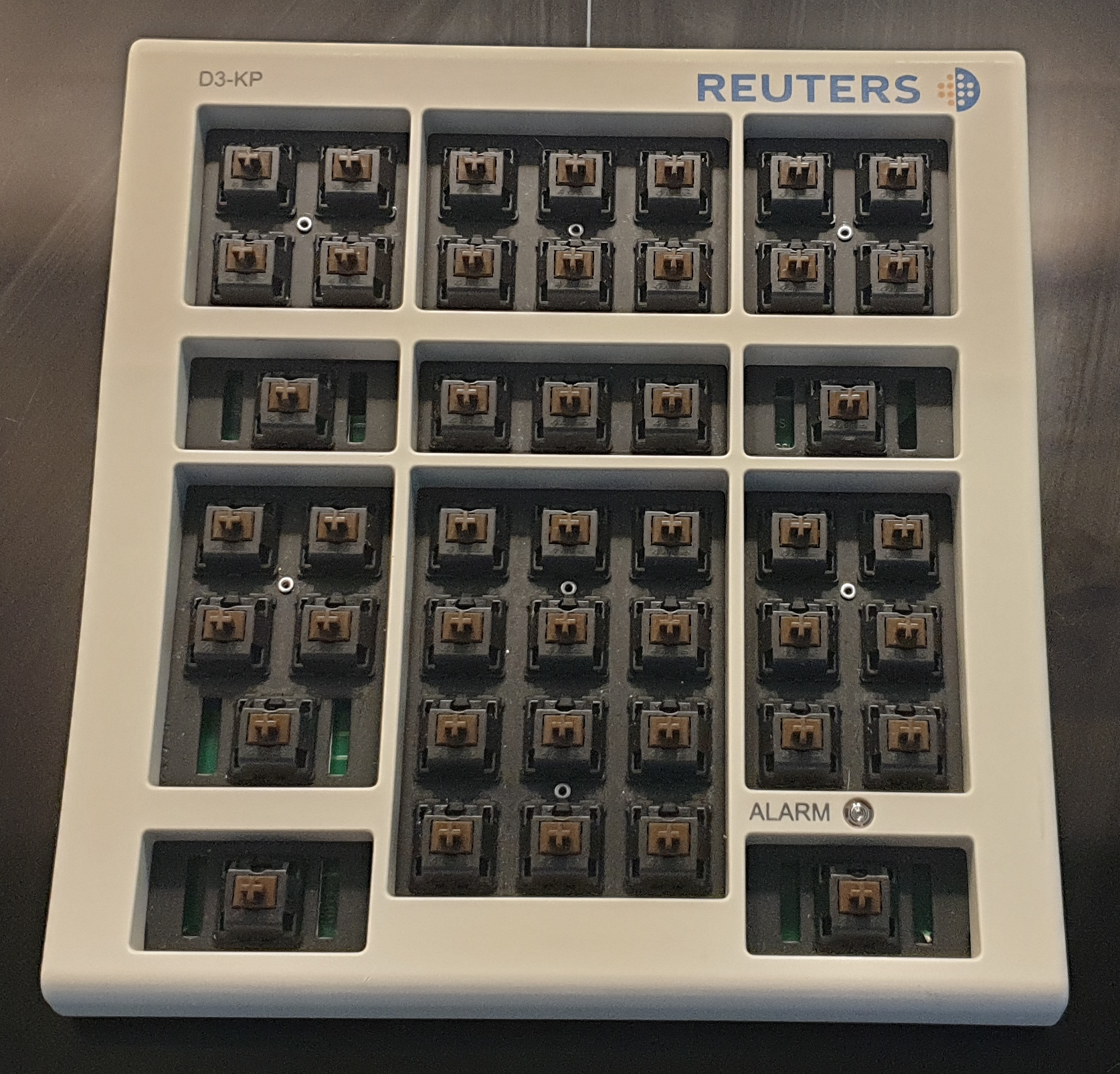
Peeling off the keycaps we see completely standard cherry browns. If we look closely we can see the pre-installed cherry diodes for the key matrix. The large MINE button shows the first strange design on this keypad, the big button are backed by 4 independent cherry switches. The top left macro key , labeled “Macro F7”, for some reason doesn’t have a diode.
Behind the switches we can see a nice black steel backplate which must be what gives the keypad the chunky feel. It weighs 682 grams, which is rather heavy for a standalone keypad. The keyboard I am typing this on (a Drop alt) is only 6 grams more.
Look at the internal hardware⌗
Time to take it apart. The shell is held together with only 9 screws, all of them easily accessible without any “warranty void” stickers; how enjoyable.
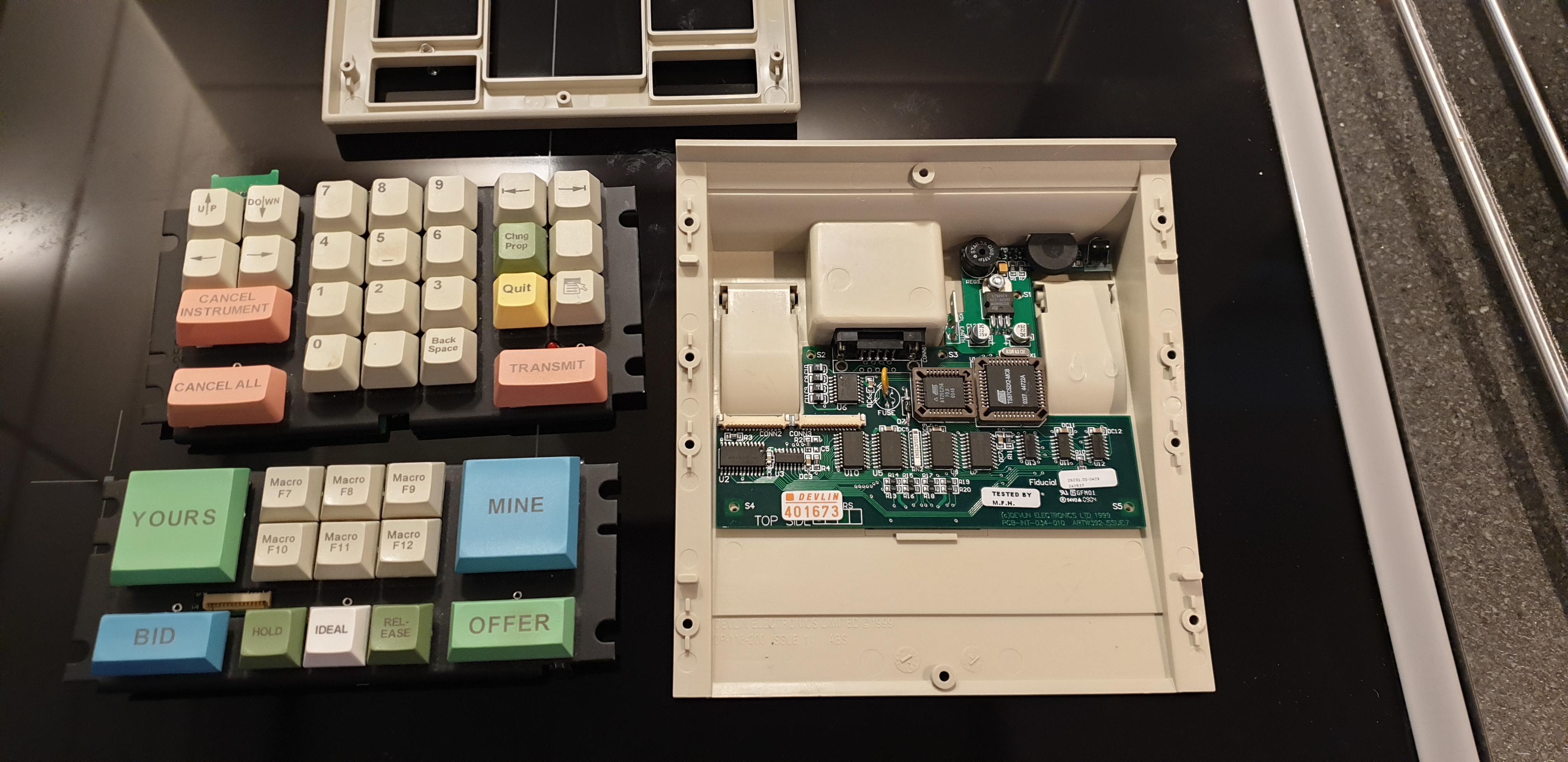
Inside, the two backplates are now free, having been held between the two shell pieces. Underneath them we find that the switches are actually soldered to two separate PCBs which then have a short wire to the mainboard. We can unhook the two picoblade connectors to completely detach the switches from the logic board. What a nice design, that’s going to make working on this board much easier.
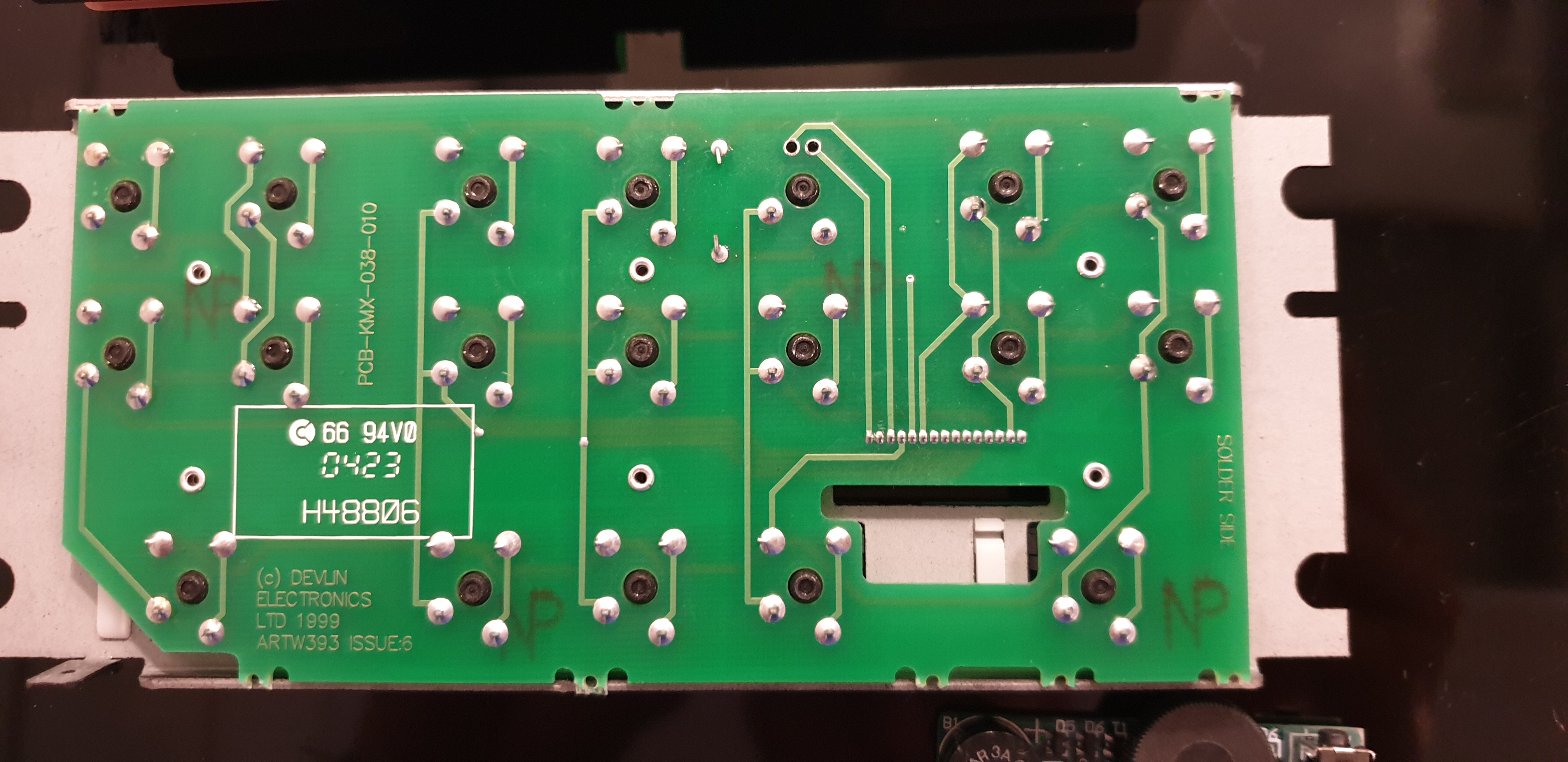
The detachable board holding the switches seem to be straight wiring. There’s no logic on there, and the switches seem to hook up in a completely normal matrix arrangement. Both the top and bottom segments seem to have space for an led, although it is missing from the top segment, where it would have been placed behind the top left macro switch. That explains why that switch doesn’t have an internal diode. It instead has an external diode on the board.
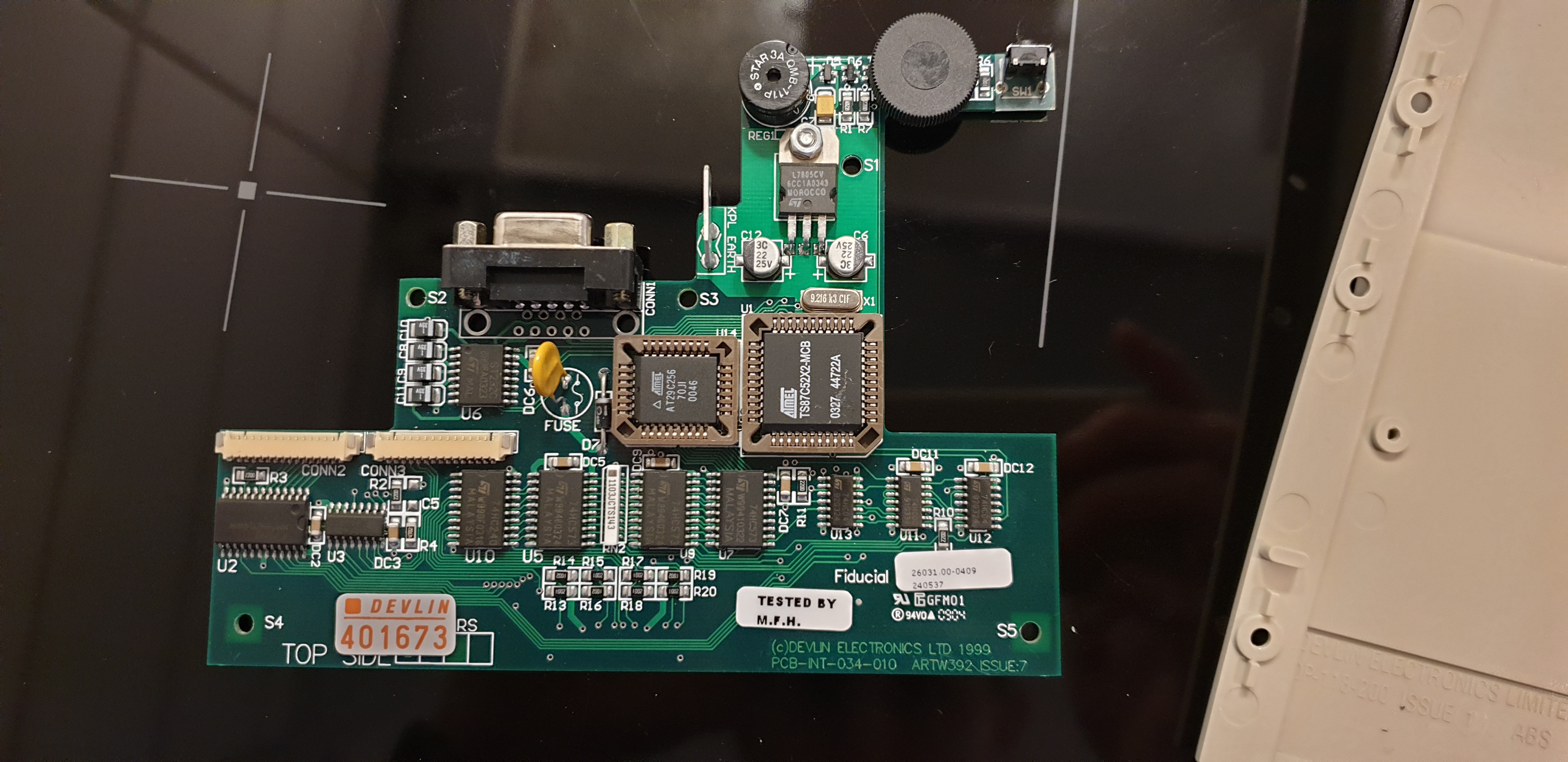
The logic board seems rather complex compared to what I would expect from an otherwise simple keyboard. At the top of the board we can see the button, the potentiometer, and strangely: a little piezo speaker. Other than that we see the processor and the memory. Finally, the board seems to contain a bunch of shift registers, memory banks, and logical inverters. I suppose the processors of the time didn’t feature as much GPIO as modern chips.
The chips are well labeled, and it’s just an ATMEGA. I could probably reprogram that and reuse it. Unfortunately, it doesn’t have any USB functionality, meaning I’d probably have to either bit-bang USB or reverse engineer the DSub and convert it. Neither sounds like the kind of thing I’d like to get into right now. That leaves me with the final option, replace the entire logic board. Since the connection between the switches and the logic board is a standard connector, A logic board replacement should be fairly straightforward, and would also let me run QMK on the keyboard.
The first step to replacing the logic board is to understand the existing connections, so we know how to hook it up to a new microcontroller.
Analysis of the electronics⌗
The first step is to determine which connections are ground. Grabbing my cheap multimeter I start probing between every pin and ground; one by one. There seems to be some connection between all pins and ground on the logic board, I’m not a master at electronics, but I presume it’s the logic components being slightly conductive. Ignoring all the high resistance connections, it seems like pin 1 and 2 are both ground.
Pin 3 is connected to one side of the LEDs, with the other side connected to ground.
Next we have to figure out how the switches are connected. The little knowledge I have about keyboards suggest they will be hooked up in a matrix. Probing the detachable boards, that is exactly what we see. The rows seem to map to pin 4-7 on both connectors (with 7 being floating on the upper board since it only has 3 rows), and the columns map to pin 8-14.
That seems to account for all the connections on both keyboard, with a catch. In order to save pins on the microcontroller (the whole point of keyboard matrices) we can construct a single, “larger” matrix by connecting the rows or columns of the two segments. Generally, you want to join the larger of the two in order to make a more square matrix. In this case the larger side is the column side, which means we can connect the column of the upper segment to the corresponding column in the lower segment to construct a single 7×7 keyboard matrix.
If we probe the original logic board, we find that the columns of both segments are indeed shorted. The keyboard is treated as a single 7×7 matrix instead of a 4×7 and a 3×7 matrices, saving those 7 pins.

Design⌗
So finally we have a few design parameters. I’m going to use the existing keyboard matrix, I’m going to replace the microcontroller, and I want to retain the reset button, the potentiometer, and the piezo speaker.
Although I could make the design on breadboard or wire it freehand, I’ve been looking for a project to try out one of the prototype PCB manufacturers. If I carefully measure the existing logic board, I should be able to get a drop in replacement with a new microcontroller, connectors and auxiliary components. That also avoids any modifications to this keypad. It’s been a long time since I last designed a PCB, but it’s worth a try.
For the microcontroller I want something that is already compatible with QMK. Although I’m a software guy, this isn’t supposed to be a software project. Since I have an 7x7 matrix I need at least 14 pins for the switches, 2 for the LEDs, 1 for the speaker, and 1 For the potentiometer. The button will be hooked up to the reset pin on the microcontroller, and therefore doesn’t require a separate GPIO pin. That’s a total of 18 pins.
The Teensy2 (a ATMEGA32U4 based development board that’s popular within custom keyboard circles) has 24 pins GPIO pins, features USB HID support, and is already fully supported in QMK. A perfect choice.
I’ve heard good things about KiCad as a Free Software PCB design offering, so I’ll be using that.
Schematic⌗
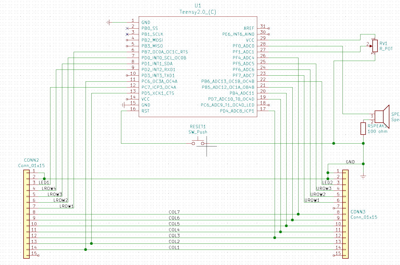
This one was an easy once since I’m mostly just connecting connectors to controller, with a few dumb components off to the side. The one notable consideration is that the potentiometer has to hooked up to a pin that is capable of ADC. Other than that it most comes down to picking pins that will make routing easier later.
Board shape⌗
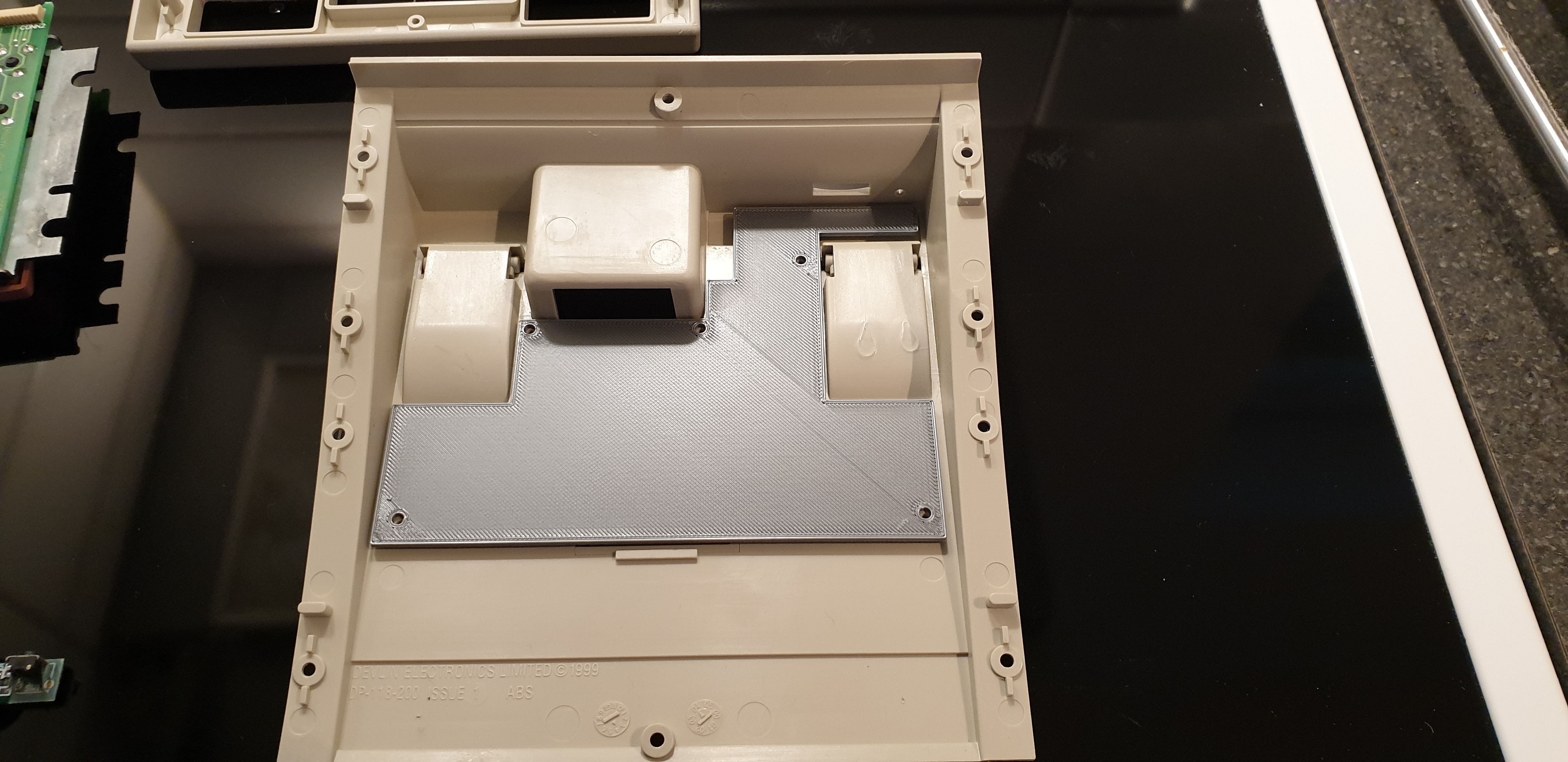
Since I’d like the board to fit the original shape I’ll have to hit the measurements pretty closely. Luckily, my 3D printer is pretty accurate, so I’ll use that to print out the shape. I’s not a perfect fit, but it’s close enough.
Board layout⌗
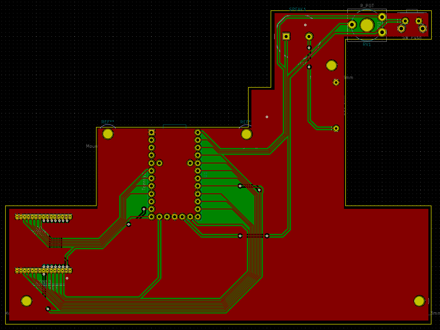
Laying out the board is fairly easy. I’ve tried to keep the connectors in roughly the same place since I want to reuse the connecting cables. The buttons and potentiometer has to go in the same spot to fit the cutouts in the plastic. The piezo could go anywhere, but why not keep it where it is. The Teensy sits where the DSub was placed on the old board. All the routing is done by hand, KiCad has some nice manual routing features, although getting going was pretty rough. I heard grounding planes are hype, so I want one.
Production⌗
For PCB manufacturer, there’s a bunch of possibilities. Rather arbitrarily I’ll just with with Aisler for this project. They seem easy, and they’re located in Europe which is nice at a time where borders all around the world are closing down.
The process is really simple. I just upload my KiCad project file, pick the options I want, and pay. 3 weeks later I get 3 boards in the mail.
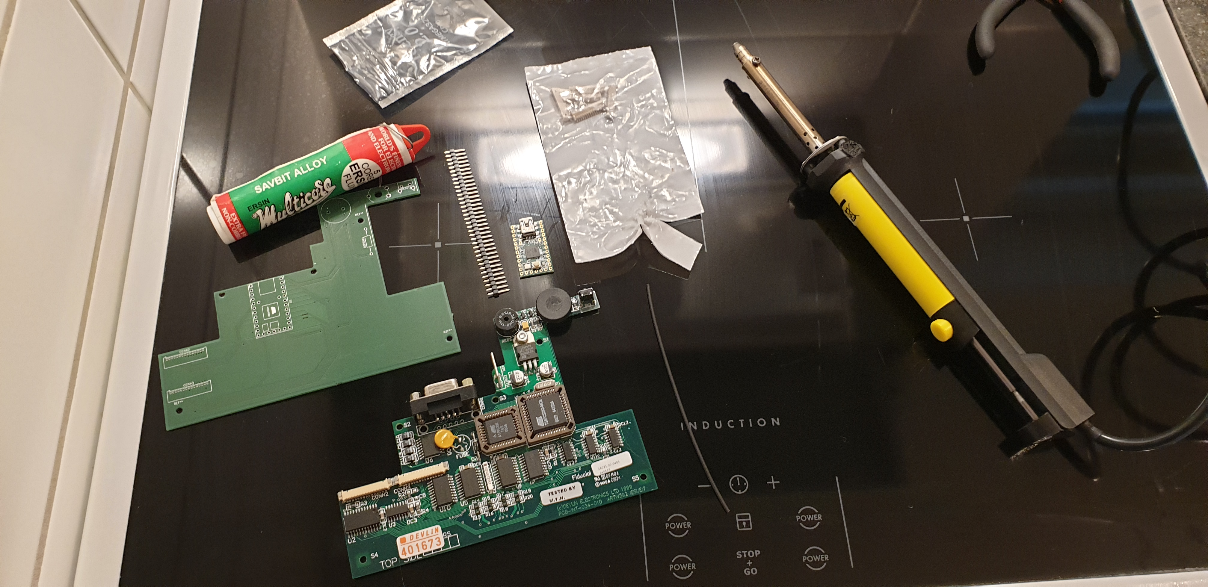
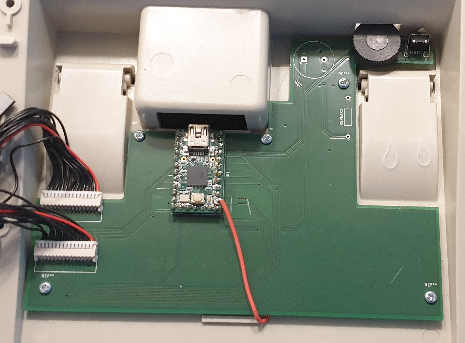
Now it’s just a matter of soldering it all together. I salvaged the button and the potentiometer from the old logic board. Unfortunately the piezo speaker didn’t survive so there will be no music from this keypad. In my design I actually flipped the picoblade connectors the wrong way. Fortunately I left myself enough room that I can just flip the connectors and they still fit.
Firmware⌗
QMK is a pretty non-controversial pick for keyboard firmware. It’s used in a ton of opensource and DIY keyboards. It’s well maintained, and very hackable. An obvious choice for this keyboard.
QMK has support for various processors and pinouts. Adding a new keyboard turns out to be pretty simple. First step is finding a keyboard that seems faily similar to the one I’m making. The ‘handwired/numpad20’ keyboard uses the Teensy2 and seems simple enough that I can tweak it for my keyboard. I won’t go into the exact configuration changes I make here, but it was as simple as defining the pins used for rows and columns, defining a new product/vendor id, and then defining the layout macro. Everything else could be left exactly as ’numpad20’. More tweaking can come in later, but for now it compiles and flashes cleanly.
Rework⌗
Booting up the keyboard for the first time The keys don’t seem to work and plugging it into my USB hub shuts off the hub. After playing around with the pc (maybe udev is broken) I touch the cable and IT’S WARM. I rip out the USB cable and start plugging away with my multimeter.
It turns out that VCC and ground is a dead short. The 3 boards I got from Aisler are all defective in the same way, they have extra unwanted vias. Aisler has a manufacturer guarantee, meaning I could probably get them to remanufacture the boards for free, but that would mean having to wait another 3 weeks. I happen to be proficient in hacks and bodges, so I know I can just cut some of the traces and rewire the connections with bodge wires. It turns out there were actually quite a few shorted connections in this board.
Conclusion⌗
After about a week worth of after work effort, and a lot of troubleshooting. I finally have a working keypad. All the keys seem to work, and the keypad even shows my custom device name in Windows and lsusb. The keyboard is complete.
If I were to do this project again I would have left way more space for the traces on my PCB. It’s so sparse, there’s really no need for my compact trace layout. I just wanted it to be neat, which turned out to be a terrible idea when I had to bodge it. Otherwise there’s not much else I would change. The keypad works beautifully, and it looks striking besides my tiny planck at work.
Now all that’s left is to rice it with some custom macros, new LEDs, and a custom 3D printed USB cover plate.